This article is derived from a lab report during my student years and is recorded here for reference. The accuracy of the content has not been verified after the experiment.
Table of contents
Open Table of contents
Overview
To construct a 16-bit adder, we can utilize Carry Lookahead Adder (CLA) components or full carry lookahead adders, connected in series. The 16-bit adder can be divided into groups of four bits, where each group uses a 4-bit carry lookahead adder, while the carry between groups is handled serially.
16-bit Adder Design
According to the full adder equations, for a 4-bit adder, the carry outputs C1,C2,C3,C4 are generated based on the following conditions:
C1C2C3C4=X1Y1+(X1+Y1)C0=X2Y2+(X2+Y2)C1=X2Y2+(X2+Y2)X1Y1+(X2+Y2)(X1+Y1)C0=X3Y3+(X3+Y3)C2=X3Y3+(X3+Y3)[X2Y2+(X2+Y2)X1Y1+(X2+Y2)(X1+Y1)C0]=X3Y3+(X3+Y3)X2Y2+(X3+Y3)(X2+Y2)X1Y1+(X3+Y3)(X2+Y2)(X1+Y1)C0=X4Y4+(X4+Y4)C3=X4Y4+(X4+Y4)[X3Y3+(X3+Y3)X2Y2+(X3+Y3)(X2+Y2)X1Y1+(X3+Y3)(X2+Y2)(X1+Y1)C0]=X4Y4+(X4+Y4)X3Y3+(X4+Y4)(X3+Y3)X2Y2+(X4+Y4)(X3+Y3)(X2+Y2)X1Y1+(X4+Y4)(X3+Y3)(X2+Y2)(X1+Y1)C0
From the equations, it is evident that each carry expression includes terms for Xi+Yi and XiYi. To simplify this, we define two auxiliary functions:
Pi=Xi+YiGi=XiYi
-
Propagate Function (Pi): This function indicates that when either Xi or Yi is 1, if there is a carry-in from the lower bit, it will definitely be passed to the higher bit.
-
Generate Function (Gi): This function indicates that when both Xi and Yi are 1, regardless of whether there is a carry-in from the lower bit, a carry-out will be produced.
Using these definitions, we can express the carry-out as:
C1C2C3C4=G1+P1⋅C0=G2+P2⋅G1+P2⋅P1⋅C0=G3+P3⋅G2+P3⋅P2⋅G1+P3⋅P2⋅P1⋅C0=G4+P4⋅G3+P4⋅P3⋅G2+P4⋅P3⋅P2⋅G1+P4⋅P3⋅P2⋅P1⋅C0
From the above expression, we see that each carry output Ci depends only on Xi, Yi, and C0. This means that there is no dependency among the carry outputs. As soon as X1 to X4, Y1 to Y4, and C0 arrive simultaneously, the carry outputs C1 to C4 can be generated almost simultaneously, alongside their respective sums.
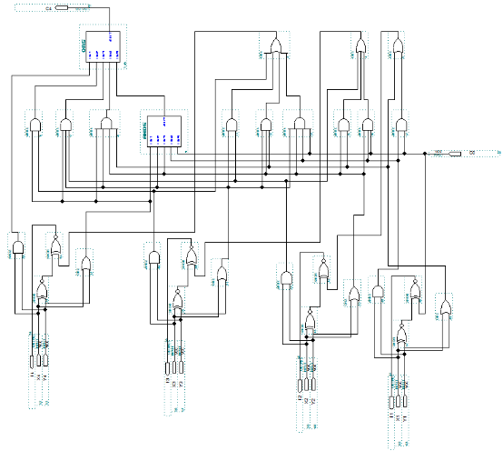
Circuit Diagram
To illustrate this concept, we can represent the wiring diagram for a 4-bit adder:
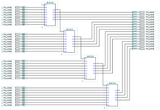
In total, for a 16-bit adder, we can connect four groups of 4-bit adders as follows:
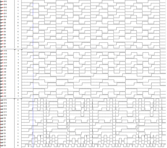
Timing Simulation Diagram
Below is a timing simulation diagram that demonstrates how the carry propagation and sum generation occur in a 16-bit adder:
Conclusion
By utilizing the principles of carry lookahead adders, we can efficiently design a 16-bit adder. This modular approach not only simplifies the complexity of the overall design but also enhances performance through faster carry generation. By effectively dividing the adder into smaller 4-bit sections, we leverage the benefits of parallel processing within the groups while managing carry propagation between groups.